Summary
This comics are intended to help in understanding the electrical on-wafer measurement for semiconductor device, process and reliability characterization. Better knowledge about device physics, a semiconductor parameter analyzer and test structures is required for accurate measurement results
- select language:
- EN

A toy for process integration engineer that is a semiconductor parameter analyzer

HP4145B is equipped with four SMUs. two VS and two Vm channels

An example how to execute Id-Vg measurement to extract the threshold voltage information

Need to understand test structures for device and process characterization

semiconductor parameter analyzer is capable of all kinds of DC I-V measurements for device and process characterization
- Scroll to:
- Ep1
- Next
Reference
- HP4145B parameter analyzer
- David Rodriguez, COE, University of California; http://www.eet.bme.hu/~mizsei/Minell/CMOS_test-structures.pdf, “Electrical testing of a CMOS baseline process”
- M. Bhushan, M.B. Ketchen, Microelectronic Test Structures for CMOS Technology
- 2017. Toshiba Memory Corporation. “Toshiba Memory Corporation Reliability Handbook.”
Related posts:
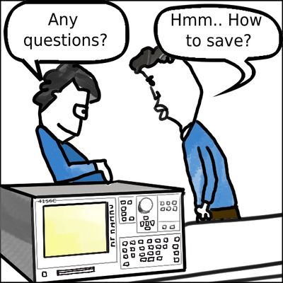 Electrical measurements to characterize semiconductor devices, processes, and reliability using Agilent 4156C parametric analyzers
 Simple and low cost test wafer for studying plasma induced wafer arcing damage
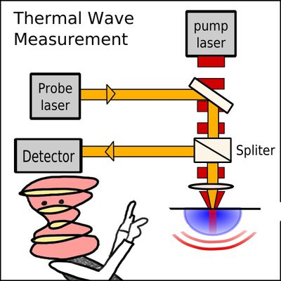 Ion beam angle uniformity wafer mapping using TW V-curves: Ep1
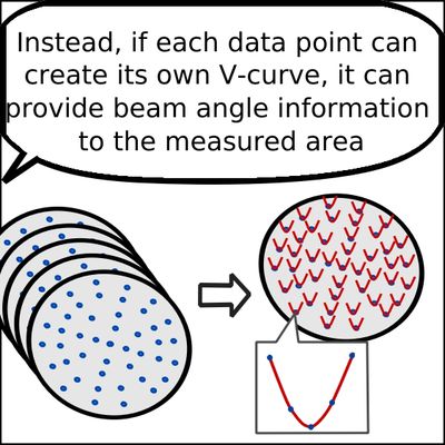 Ion beam angle uniformity wafer mapping using TW V-curves: Ep2
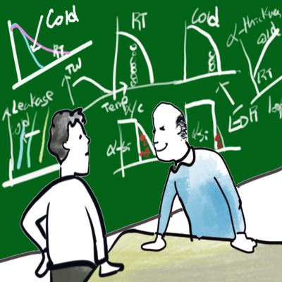 Implant damage control and junction leakage measurement
 Things to know before doing E-Beam lithography at Harvard CNS: Ep2
Leave a Reply