Summary
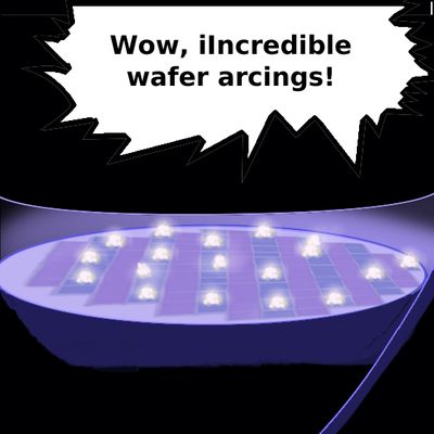
Wafer arcing is a response to particular wafer surface structure geometry as well as plasma instability. Therefore, the type of wafer surface structure can be an important factor for process optimization to reduce the arcing frequency. All plasma processing systems need to have real-time micro-arcing detection and analysis capability to prevent further arcing. .
- select language:
- EN

A common problem that exists for plasma sputtering, PECVD deposition, plasma reactive ion etching, plasma doping or plasma immersion ion implantation is to avoid plasma arcing called “wafer arcing” or “micro-arcing”. The problem leads to device destruction, wafer yield loss, reliability failure, and ruin of process chamber.

Wafer arcing is a response to particular wafer surface structure geometry, plasma chamberwall condition and plasma instability. Therefore, the type of wafer surface structure can be an important factor for process optimization to reduce the arcing frequency.

In the case of a photoresist wafer, heavy wafer arcing occurs in a defect surface region such as PR cracks due to water penetration in the resist film. It should be noted that the degree of cracking on the PR surface depends on the quality of photoresist

In the case of a photoresist wafer, heavy wafer arcing occurs in a defect surface region such as PR cracks due to water penetration in the resist film. It should be noted that the degree of cracking on the PR surface depends on the quality of photoresist.
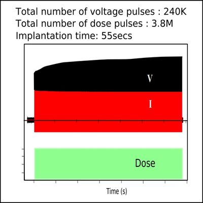
Arcing occures at microseconds so high speed data acquisition is suggested to detect arcing events. Earlier detection of micro-arcing is key to prevent further arcing that will result in wafer damage, process chamber damage, contamination, yield loss and reliability failure.
- Scroll to:
- Ep1
- Next
Reference
- Ma, S., et al. “Backend dielectric etch induced wafer arcing mechanism and solution.” 2003 8th International Symposium Plasma- and Process-Induced Damage.
- Arshad, Muhammad Z., and Sang J. Hong. “In-Situ Detection Method of Abnormal Plasma Discharge in Plasma-Assisted Deposition Processes.” Transactions on Electrical and Electronic Materials, vol. 19, no. 2, 2018, pp. 96-100.
- “Micro-Arcing During High-Density Plasma Chemical Vapor Deposition | Applied Materials.” Applied Materials | Semiconductor, Display and Solar, www.appliedmaterials.com/nanochip/nanochip-fab-solutions/october-2016/micro-arcing.
Related posts:
 Plasma doping/PIII advantages over beamline implantation
 Dose accuracy in plasma doping
 Implant pulse parameters to monitor plasma ion implantation systems for fault detection and process control
 Wafer surface structure sensitivity to plasma doping induced arcing
 Ion beam angle uniformity wafer mapping using TW V-curves: Ep1
 Ion beam angle uniformity wafer mapping using TW V-curves: Ep2
Leave a Reply