Summary
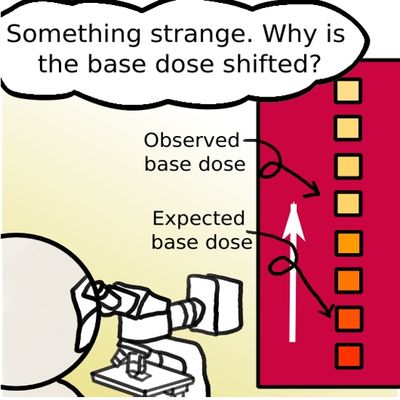
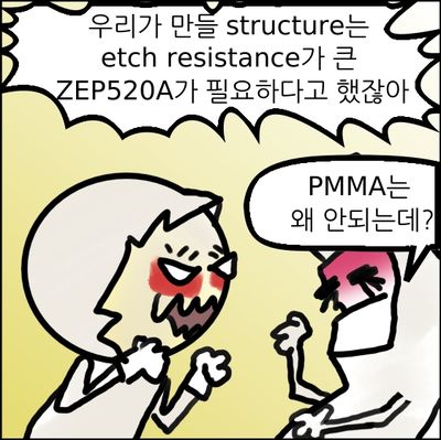
PMMA and ZEP520 are the most popular positive E-beam resists with high resolution capability. ZEP520 is well-known for high sensitivity and etch durability but is expensive. Note that The resist performance, contrast, sensitivity and resolution depends strongly on the development process.
- select language:
- En
- KR

Public parking around the Harvard CNS is not easy. To make your visit easy buy a daily visitor parking permit online in advance and print out it. The 52 Oxford Street Garage is the closest to the Harvard CNS.

Harvard CNS users should register IRIS eye scan access system to enter the cleanroom

There are two popular positive E-beam resists. ZEP520 is very expensive compared to PMMA

Check the spin curves of the E-beam resist you use. Your desired resist thickness will give the spin speed

The resist performance, contrast, sensitivity and resolution depends strongly on the development process. It is suggested to understand the different developers for PMMA and ZEP520.
Related posts:
 하버드대 CNS 나노팹에서 소자제조 – Ep1
(Getting ready)
Nanofabrication at Harvard CNS : E-beam resist – Ep1( Getting ready)
 E-Beam Lithography Resists (2)- 하버드대 CNS 나노팹에서 소자제조 – 3화
 Nanofabrication at Harvard CNS : E-beam resist – Ep3
 Things to know before doing E-Beam lithography at Harvard CNS: Ep1
 Wafer surface structure sensitivity to plasma doping induced arcing
Leave a Reply