Summary
Migration toward next nod scaling of semiconductor device forces the equipment manufactures to develop new process technology to meet the more stringent specifications and to overcome the process challenges of the new technology nod. To ensure the process quality of newly developed technologies, customized test structures are developed. In Boston region Harvard CNS is used for nanofabrication of prototypes.
- select language:
- EN
- KR

A prototyping project was approved

A design layout of ptototye structure

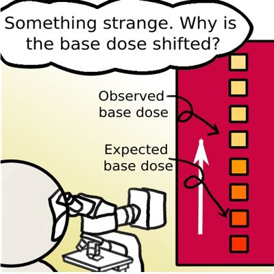
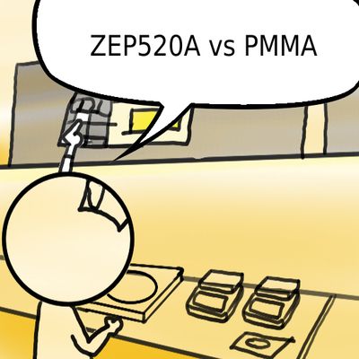
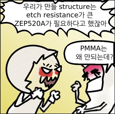
Process challenges in nanofabrication of the test structures

Gold improves image contrast in SEM
- Scroll to:
- Ep1
- Ep2
Related posts:
 하버드대 CNS 나노팹에서 소자제조 – Ep1
(Getting ready)
 E-Beam Lithography Resists (2)- 하버드대 CNS 나노팹에서 소자제조 – 3화
 E-Beam resist – Nanofabrication at Harvard CNS – Ep2
 Nanofabrication at Harvard CNS : E-beam resist – Ep3
 Things to know before doing E-Beam lithography at Harvard CNS: Ep1
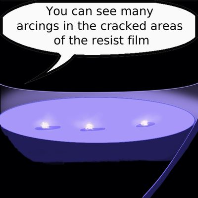 Simple and low cost test wafer for studying plasma induced wafer arcing damage
Leave a Reply