Summary
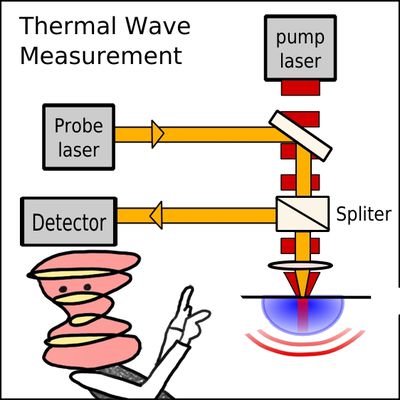
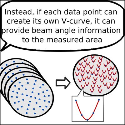
Beam angle information from nanoscale electrical test structure can provide high resolution wafer maps of the horizontal and vertical incident beam angle and angle spread, and beam parallelism across a wafer.


Precise angle control requirements of both horizontal and vertical direction become more stringent with more advanced nodes. Next is about how an implanter controls the incident beam angles as closed-loop method.


It is worthy to note that the above methods are based on bare wafer. Nanoscale device wafer will provide more actual beam angle information.


Related posts:
 Ion beam angle uniformity wafer mapping using TW V-curves: Ep1
 Ion beam angle uniformity wafer mapping using TW V-curves: Ep2
 Implant damage control and junction leakage measurement
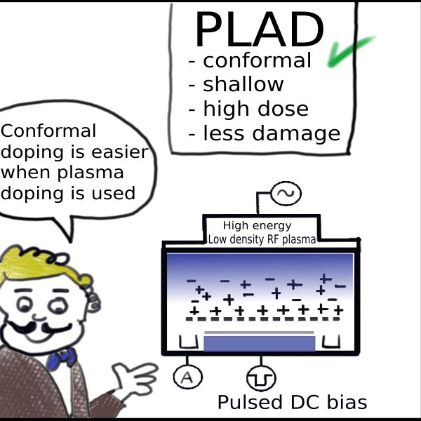 Conformal Doping Test Structure for PLAD process qualification
 Mapping wafer temperature spatial distribution
 Wafer surface structure sensitivity to plasma doping induced arcing
Leave a Reply