Summary
Test structure method to probe doping conformality enables the automated measurement of nano-scale sidewall electrical depth profile and provides a wafer map on the degree of sidewall conformal doping.


If you want a full comic script please contact at skyonsky@gmail.com


Related posts:
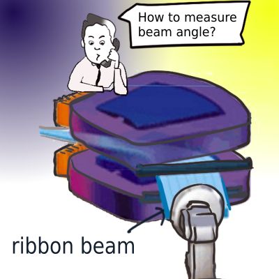 Test Structures to measure the Implant Beam Angle for accurate beam control
 Implant damage control and junction leakage measurement
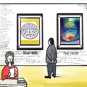 Mapping wafer temperature spatial distribution
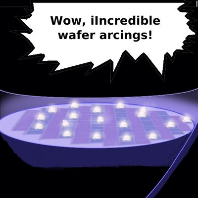 Wafer surface structure sensitivity to plasma doping induced arcing
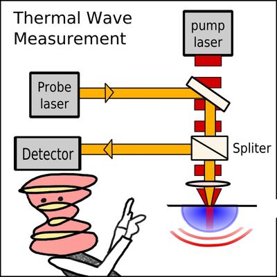 Ion beam angle uniformity wafer mapping using TW V-curves: Ep1
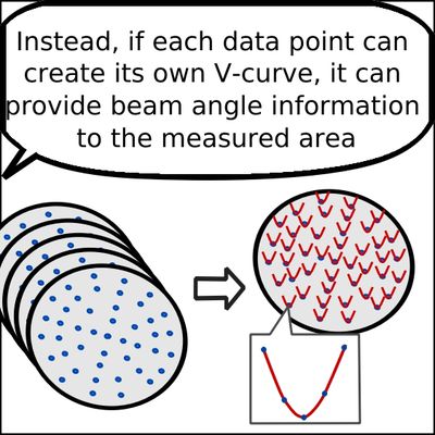 Ion beam angle uniformity wafer mapping using TW V-curves: Ep2
Leave a Reply