Summary
Semiconductor parameter analyzers have a wide range of electrical measurement capabilities and are used to characterize semiconductor devices, processes, and materials, and to text reliability in the semiconductor industry. Profound knowledge about an analyzer is helpful to accelerate research and development.
- select language:
- EN

Semiconductor parameter analyzers are all-in-one tools used for electrical characterization of materials, semiconduc-
tor devices and processes. The analyzer is one of essential tools that process integration engineer must learn.

Agilent 4156C is equipped with 8 channels (four SMUs, two VS and two Vm channels) and can perform three types of measurements such as sweep, sampling and QS-CV measurement

An example how to execute Id-Vg measurement to extract the threshold voltage information

Set up measurement parameters, display and user functions

Interfacing softwares like Metrics ICS and Easyexperts are used to control the parametric analyzer. Using a Pusle Generator Expander AC/DC stress test can be performed.

Semiconductor parameter analyzer, 4156C is capable of a wide range of DC IV/CV measurements for device and process characterization, reliability test, and failure analysis
- Scroll to:
- Ep1
- Ep2
Reference
- “Agilent 4156C Programmer’s Guide”
- “Measuring MOSFET properties”
- 2017. Toshiba Memory Corporation. “Toshiba Memory Corporation Reliability Handbook.”
- “Metrics ICS software”
- “EasyEXPERT Software Users guide”
- Alan Doolittle. School of Electrical and Computer Engineering, Georgia Institute of Technology. “Semiconductor Device and Material Characterization”
Related posts:
 Electrical measurements to characterize semiconductor devices, processes, and reliability using HP 4145B parametric analyzers
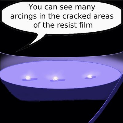 Simple and low cost test wafer for studying plasma induced wafer arcing damage
 Ion beam angle uniformity wafer mapping using TW V-curves: Ep1
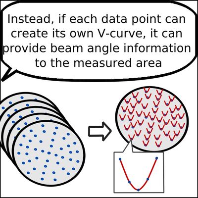 Ion beam angle uniformity wafer mapping using TW V-curves: Ep2
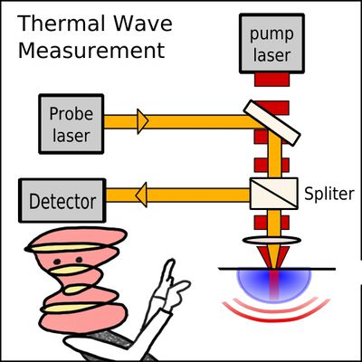
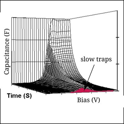 3D C-V measurement to detect slow traps
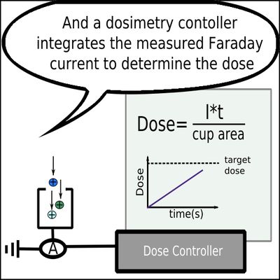 Dose accuracy in plasma doping
Leave a Reply