Summary
Plasma induced wafer arcing is sensitive to hardware condition as well as wafer surface structure, such as pattern layout, feature density and wafer edge roughness
- select language:
- En

The effect of photoresist edge roughness on plasma induced wafer arcing

The higher the feature density, the greater the wafer arcing risk

The plasma induced wafer is sensitive to hardware condition as well as pattern layout

Active diode test structure sensitivity to plasma doping induced wafer arcing

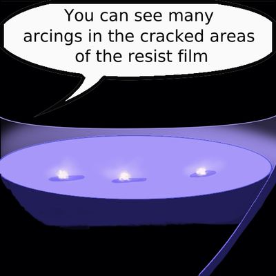
Too much charge accumulation on oxide causes oxide breakdown, resulting in wafer arcing

Antenna test structure sensitivity to plasma doping induced wafer arcing

Plasma induced charging is responsible for wafer arcing. Therefore, good control of plasma induced surface charging can avoid wafer arcing. The wafer arcing is sensitive to the antenna test structure
- Scroll to:
- Ep1
- Ep2
Reference
- Ma, S., et al. “Backend dielectric etch induced wafer arcing mechanism and solution.” 2003 8th International Symposium Plasma- and Process-Induced Damage
- MA, S. “Plasma Induced Charging Damage: From An Semiconductor Equipment Vendor Point of View.” pdfs.semanticscholar.org/presentation/a96b/ee9ad164569cfa51d2847dd83d150b000829.pdf
Related posts:
 Plasma doping/PIII advantages over beamline implantation
 Dose accuracy in plasma doping
 Implant pulse parameters to monitor plasma ion implantation systems for fault detection and process control
 Simple and low cost test wafer for studying plasma induced wafer arcing damage
How to monitor plasma ion implantation process for fault detection?
Simple and low cost test wafer for studying plasma induced wafer arcing damage
How to monitor plasma ion implantation process for fault detection?
 NI-Diadem for plasma doping process monitoring
Leave a Reply