• Skip to primary navigation
  • Skip to main content

Vonoff

SkyKo Comics and videos about Semiconductor and nanotechnology | 반도체 만화

  • HOME
  • COMICS & VIDEOS
  • ABOUT
  • CONTACT

Main Content

SkyKO comics about semiconductor

Comics
about
Semiconductor

Have your technologyunderstood

Have your technology understood

I can help you to create custom comics to explain your technology in a memorable way

Featured Comics:

View All
Memory system evolution

Making faster memory system

Ep1

View more

A trip down memory lane-#1

lithography trends

Trends of lithography

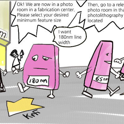
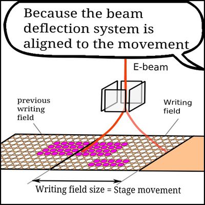
Lithography technology to EUV

View more

Trends of lithography

implant damage conrol-cold implantation

Implant damage control

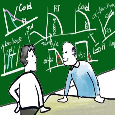
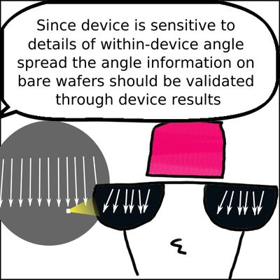
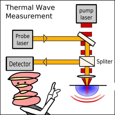
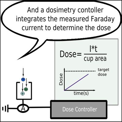
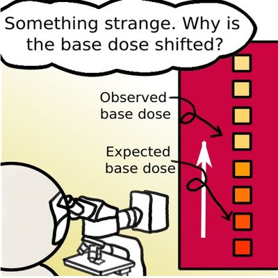
by using cold and cluster ion implant

View more

Cold & cluster ion implant

Implant beam angle control

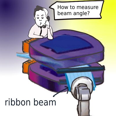
Test structure for beam angle measurement

View more

Implant beam angle measurement

Recent Comics:

View All
thumnail of Coronavirus self isolation in Korea

Self-isolation in Korea-Day1

Sky Comics about Lao Sinh or Lao skirt-Ep1-thumnail

Laos travel comics:
Lao skirt, lao sinh

thumnail of skyonsky Episode 4 -p1- skyko comics about life story

Life story comics-SkyOnSky Ep4: Move to NZ

E-beam lithography-Ep4-thumnail-1

Things to know before doing E-Beam lithography at Harvard CNS: Ep2

Elionix ELS-F125 Electron Beam Lithography System at Harvard CNS

Things to know before doing E-Beam lithography at Harvard CNS: Ep1

High resolution ion beam angle uniformity wafer mapping in implantation by using thermal wave(TW) V-curves-thumnail3

High resolution ion beam angle uniformity wafer mapping by using thermal wave-Ep2

ion beam angle measurement using thermal wave-TW measurement theory-thumnail

TW measurement theory-High resolution ion beam angle uniformity wafer mapping by using thermal wave-Ep1

plasma induced wafer arcing

wafer level test structure sensitivity to plasma doping induced wafer arcing

a thumnail about influence of wafer surface structure on plasma induced micro-arcing

Impact of wafer surface structure on plasma induced micro-arcing

Monitoring plasma ion implantation systems for fault detection and process control-thumnail-1

Monitoring plasma ion implantation systems for fault detection and process control

plasma-doping-dose-accuracy-thumnail2

Plasma-doping-dose-accuracy

plasma doping advantages over beamline-thumnail

Plasma doping advantages over beamline

semiconductor_electrical_characterization_ep2-thumnail1

Electrical measurement for semiconductor device and process characterization

semiconductor device and process characterization with a parameter analyzer

semiconductor electrical measurement with a parameter analyzer

E-Beam resit characterization-nanofabrication_at_havardcns-ep3-thumnail

E-beam resist(2)-Nanofabrication at Harvard CNS-Ep3

nanofabrication at Harvard CNS-Ep1(kr)

Getting ready-Nanofabrication at Harvard CNS-Ep1

support

To help sponsor my work

Sponsor
  • skyonsky@gmail.com
  • About
  • Comics

All work © Sky KO-