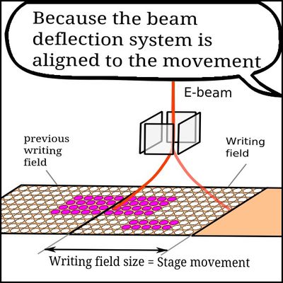
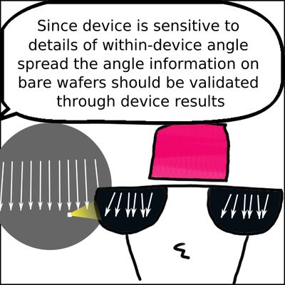
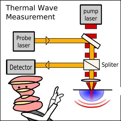
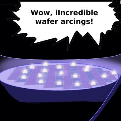
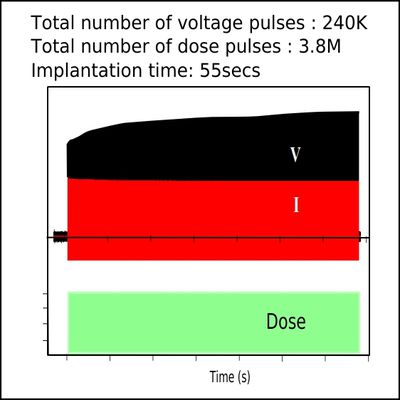
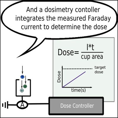
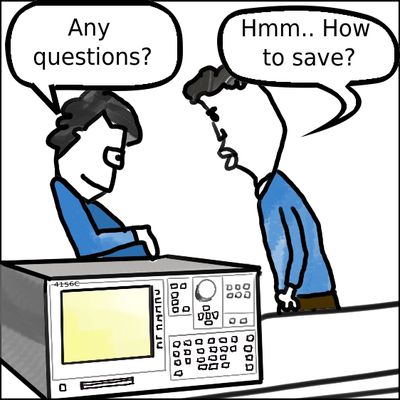
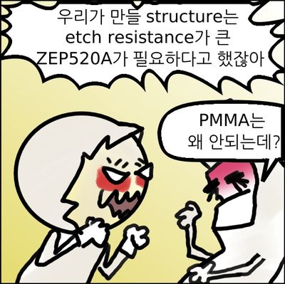
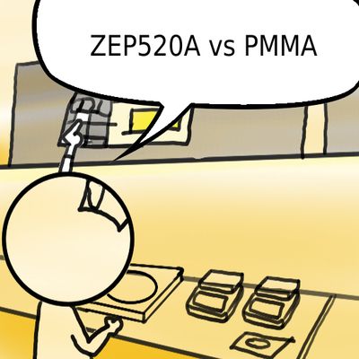
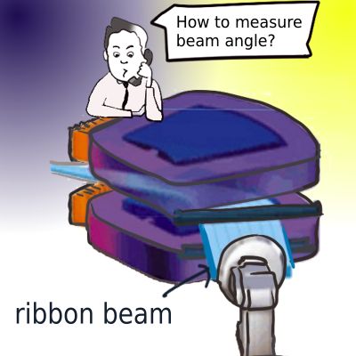
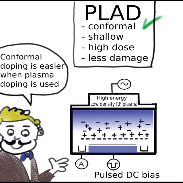
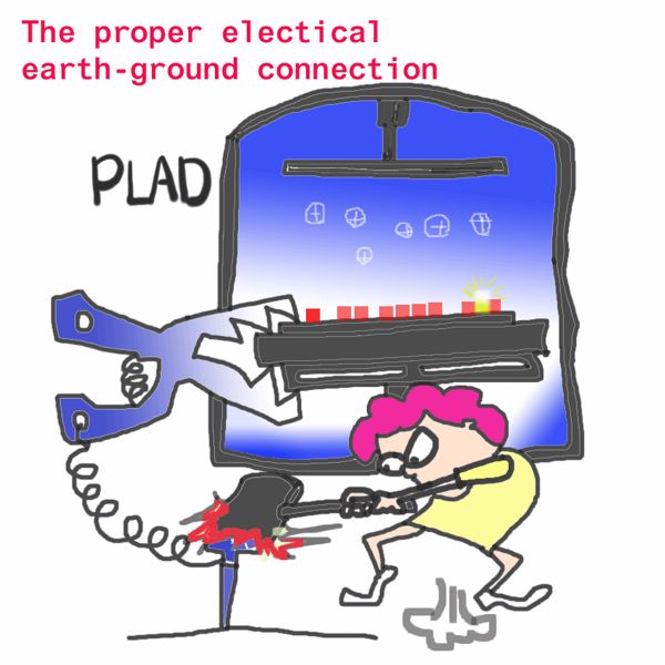
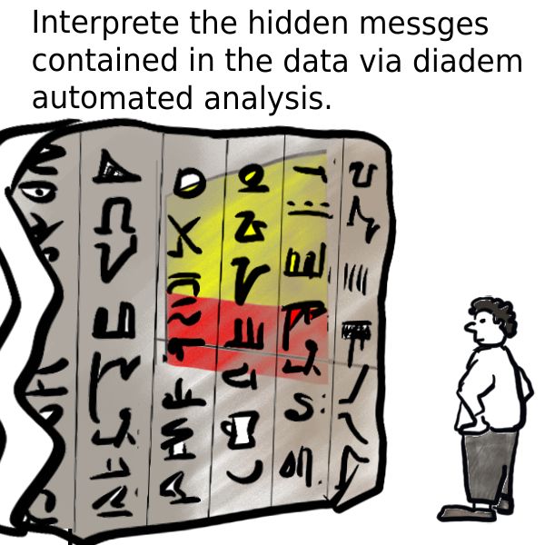
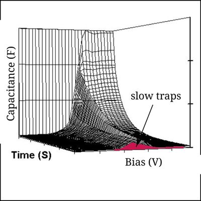
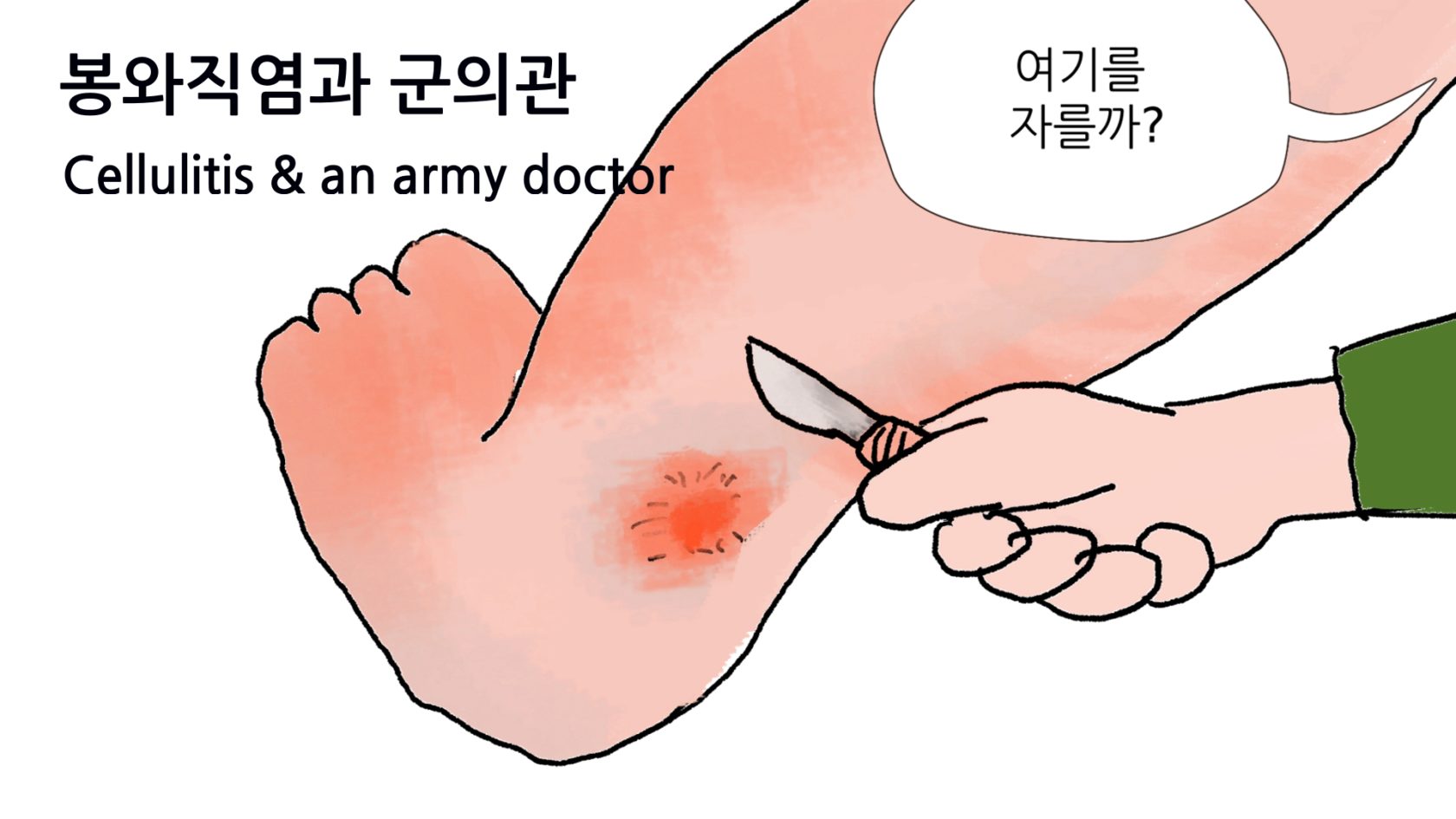
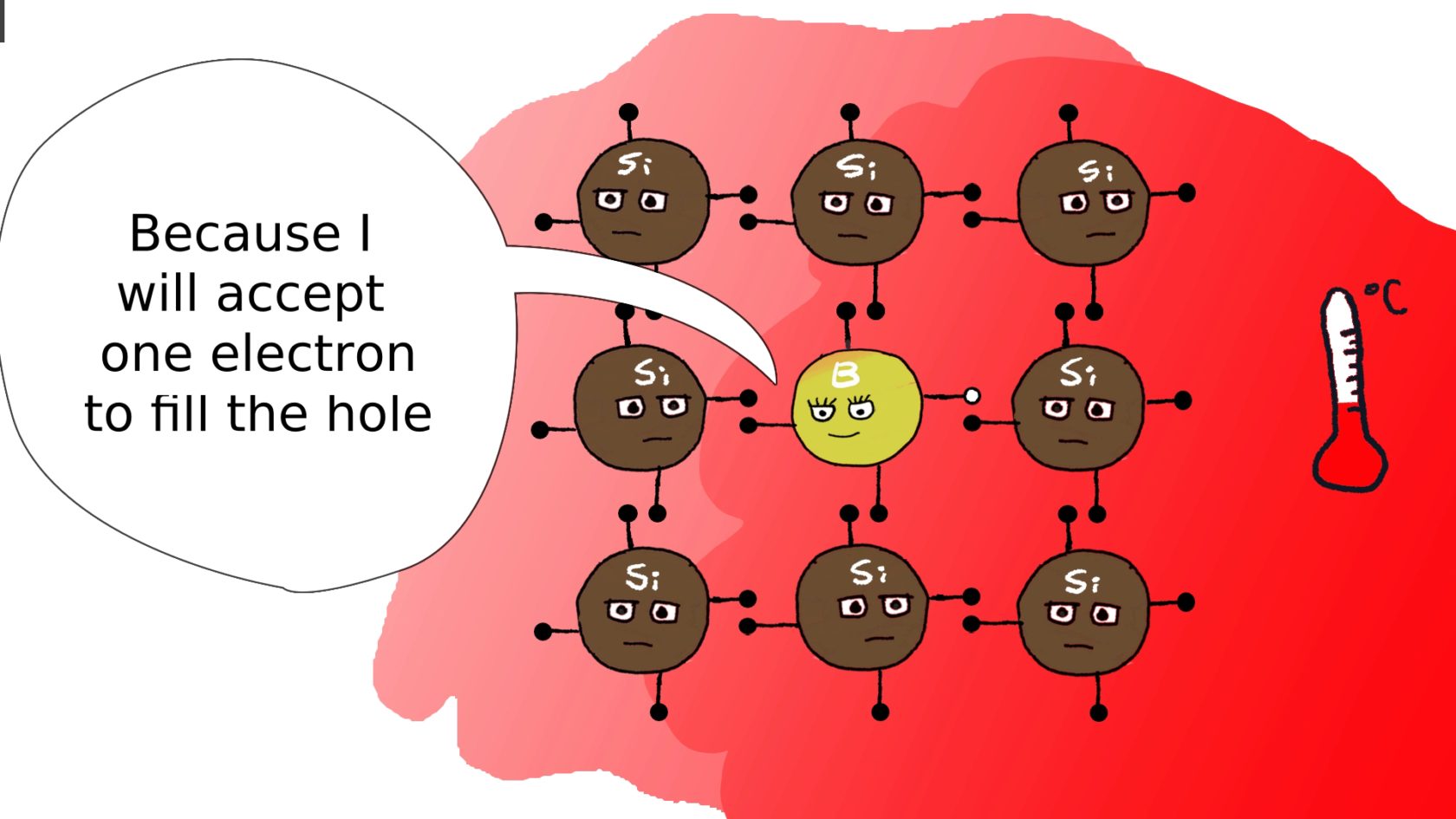
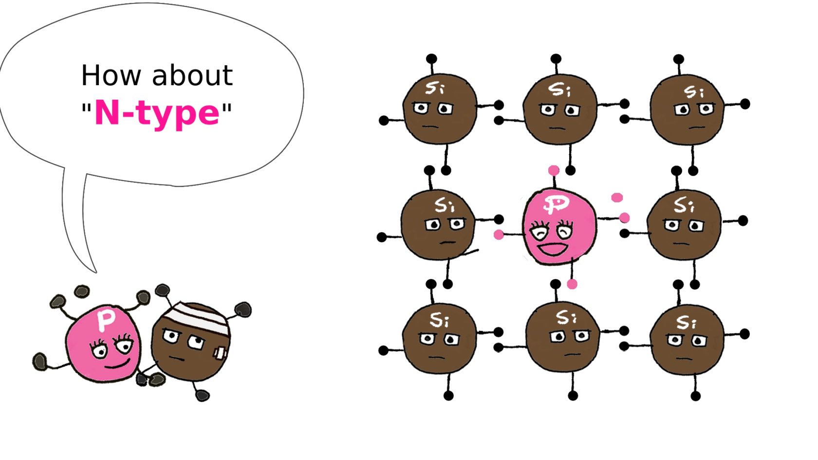
COMICS SkyKo Comics and Animations media type any comics video subject any semiconductor life semiconductor category any ebeam implant plad metrology memory beam angle conformal photo litho surface cleaning Things to know before E-beam litho at Harvard CNS-Ep2E-beam lithography basics-Ep2: Minimizing stitching errors Things to know before E-beam litho at Harvard CNS-Ep1E-beam lithography basics:Ep1 How to veryify ion beam angle accuracyHigh resolution micro-uniformity map of beam angle provides beam angle detailsEp.2 Ion beam angle performance monitoringHow to create high resolution beam angle uniformity mapEp.1 Plasma doping induced arcingThe influence of surface structure and micro-arcing detection Plasma wafer arcingTest structure sensitivity to plasma induced wafer arcing How to monitor plasma doping processHigh speed data acquisition and large data analysis Dose accuracyIs dosimetry dose same as retained dose in plasma doping? PLAD .vs BeamlinePLAD advantages over beamline Electrical measurementElectrical measurement with parameter analyzer used for device and process characterization DC-IV measurementWhat is semiconductor parameter analyzer like 4156C that has a wide range of electrical measurement capabilities nanofabrication at harvard CNS-Ep3 (E-Beam resist(2) Understand the characteristics of E-beam resists first for successful EBL Nanofabrication at harvard CNS-Ep.2 (E-beam resist) Comparison of E-beam resists, Zep520A and PMMA Nanofabrication at Harvard CNS-Ep1(Prototyping) Getting ready A trip down memory lane -#3: DRAM vs. emerging memories Ep3 (EN,KR): The resistance-based non-volatile memories(NVM), PCRAM, STT-MRAM and ReRAM are introduced to the memory heirarchy A trip down memory lane -#2: : The sorrow of DRAM scaling challenge Ep2 (EN,KR): Can DRAM overcome its physical scaling limit and stay relevant? A trip down memory lane -#1: Memory to reduce latency gap Ep1 (EN,KR): Processors and memory have always differed in priorities Lithography Trends What has happened to force the lithography roadmap accelerate? Implant damage controlEffect of cold and cluster implantation on junction leakage Implant beam angle control Test structure for beam angle measurement Test structure method to probe doping conformality Automated measurement of nano-scale sidewall electrical depth profile Cold implantation wafer temperature uniformity A custom-made probe wafer to map wafer temperature spatial distribution SC1 wet clean effectSC1 clean induced device yield drop PLAD development Key process issues with PLAD High speed data acquisition In-situ monitoring for fault detection using NI-Diadem Electrical measurementsemiconductor device and process characterization 3D C-V technique Visualization of slow traps of MOS How do you want be remembered? Ep1 Good people I still remember- A military doctor and Cellulitis-Korean army several decades ago How do you want be remembered? Ep2 Good people I still remember- Boston ajeossi-the best buns and coffee-Korean army several decades ago Laos Skirt or Lao Sinh Laos travel story about Laos traditional customs: Laos Skirt or Lao Sinh – Ep1:skyko comic animation What is P-type? What is P-type, intrinsic and extrinsic semiconductor?:semiconductor comic animation-Ep2 What is N-type? What is N-type semiconductor? Semiconductor comics animation-Ep1 Lao skirt – Sihn: Ep1 Laos traditional custome-Sinh