Summary
The 3D C-V technique is a simple method to measure the energy and concentration profile of the slow traps located in the oxide near the Si-
SiO 2 interface.

What is 3D C-V? It is a measurement technique developed by Sky Ko and a Kiwi scientist to visualize the slow traps of MOS structure. It is a simple method to characterize the distribution of near interface oxide traps by measuring the charge of the MOS capacitor in real-time.

3D C-V is comprised of the continuous charge waveforms of MOS capacitor in each bias from accumulation to inversion.

There are several types of oxide charges. #D C-V techniques is used to measure oxide charges and interface traps in MOS structure.

The existence of slow traps causes the gradual increase in capacitance. Therefore, charge waveform is useful to simply diagnose them and the leaky MOS. 3D C-V technique uses “Feedback charge methode” to measure the charge waveform of MOS capacitor.

Once 3D C-V curves are created slow traps are easily observed in an energy distribution. 3D C-V technique provides information simultaneously on trap density, their energy distribution and trap response time.
Related posts:
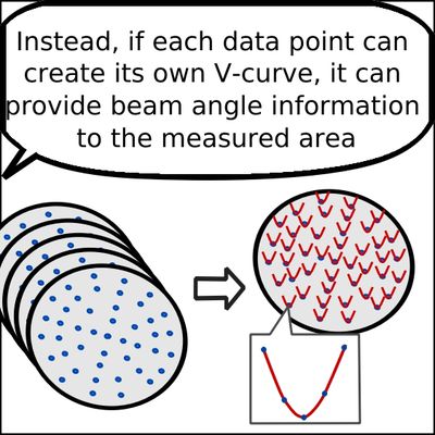
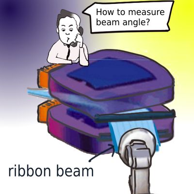 Test Structures to measure the Implant Beam Angle for accurate beam control
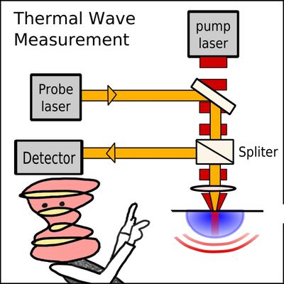
 Implant damage control and junction leakage measurement
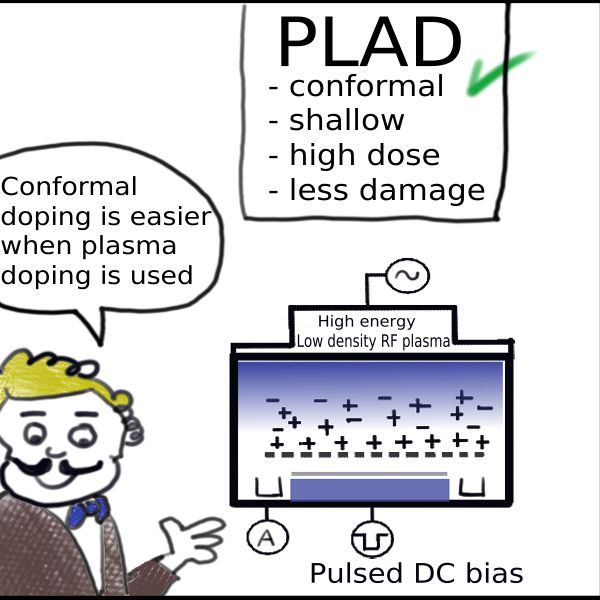 Conformal Doping Test Structure for PLAD process qualification
 Plasma doping/PIII advantages over beamline implantation
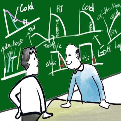
 Ion beam angle uniformity wafer mapping using TW V-curves: Ep1
 Ion beam angle uniformity wafer mapping using TW V-curves: Ep2
Leave a Reply