Summary
This comic explains what you need to know before doing electron beam lithography with Elionix systems at Harvard CNS: system, beam spot size, shot pitch, vector scan, and pattern design strategic.
- select language:
- En

There are two Elionix electron Beam Lithography Systems at Harvard CNS: ELS-F125 and 7000

The key points of electron optics system and specification of ELS-F125

How to write a pattern with e-beam and the beam spot size that is dependent on beam current, aperture, acceleration voltage and WD

E-beam current and aperture determine the ebeam spot size. Choose them depending on the feature size that you will write

How to define the shop pitch, also called step size. You first need to set the beam position resolution.

How to set the position resolution and the shot pitch(step size)
 P7
P7Make sure to design pattern so that all shapes snap to some multipe of the shot pitch. Otherwise the pattern does not fit to the shot pitch. The X and Y shot pitchs don’t need to be the same.

There are two type of e-beam scan methods to write the pattern: Vector scan and Raster scan.

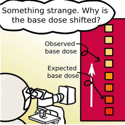
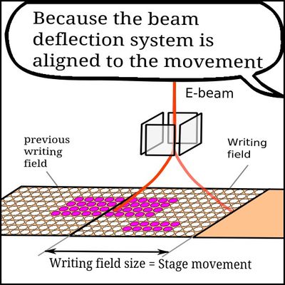
With vector scan there is no stage movement if the pattern is within the write field. The 2D deflector system deflects the beam to control its position of the beam. However, any pattern larger than a sing writing field is divided into multiple fields. The stage has to move to the next after each write field. Thses stage moves gives rise to stitching errors unless the system is well-calibrated.
- Scroll to:
- Ep1
- Next
Reference
- Cen, Shawn W, et al. High-energy Electron Beam Lithography for Nanoscale Fabrication. INTECH Open Access Publisher, 2010.
- Chen, ChiiDong. “Advanced Device Fabrication Techniques.” Institute of Physics, Academia Sinica. Lecture.
- “Elionix Electron Beam Lithography System ELS-G100.” Wisconsin Center for Microelectronics (WCAM), UW-Madison College of Engineering, wcam.engr.wisc.edu/Public/Tools/Lithography/Elionix%20ELS-G100%20Operating%20Procedure.pdf.
- “Introduction to ebeam Lithography.” Materials Research Science and Engineering Center – UW–Madison, mrsec.wiscweb.wisc.edu/wp-content/uploads/sites/282/2018/04/Yong-Sun.pdf.
- “Electron-Beam Lithography Training.” Welcome | Yale Institute for Nanoscience and Quantum Engineering, nano.yale.edu/book/export/html/213.
- “ELIONIX ELECTRON BEAM LITHOGRAPHY SYSTEM ELS-G100.” Wisconsin Center for Microelectronics (WCAM), wcam.engr.wisc.edu/Public/Tools/Lithography/Elionix%20ELS-G100%20Operating%20Procedure.pdf.
- “EOL JBX-9300FS Electron Beam Lithography System Training.” Nanolithography, www.nanolithography.gatech.edu/JEOL_JBX-9300FS_Training.pdf.
- “EBeam Basics 1.” Washington Nanofabrication Facility, Electron Beam Lithography, ebeam.mff.uw.edu/ebeamweb/doc/exp/exp/exposure_basics_1.html.
- “E-beam Lithography.” Vor Brodie and Julius Muray ”The Physics of Micro/Nano-Fabrication”, fy.chalmers.se/~yurgens/FKA196/lectures/E-beam%20lithography.pdf.

Leave a Reply