Summary
A custom-made probe wafer with RTD sensor provides wafer temperature spatial distribution map by measuring transient temperature distribution in a silicon wafer. This can validate wafer temperature control for cold implantation.

Cryo implantation creates nonuniform wafer temperature distribution across a wafer. Based on Thermal-Wave(TW) contour map it looks like that it is the spatial temperature gradient from the lowest temperature region that contacts cryo source

How to build a custom-made cheap 300mm temperature probe wafer with RTD sensors

Real-time wafer temperature of a number of RTD sensors is measured by using data acquisition. Analysis of heat transfer to map wafer temperatures visualizes the progress of heat transfer acrros a wafer

This method provides useful information on temperature differentials across a wafer and correlation with thermal wave map and results from a commercial probe wafer such as KLA-Tencor SensArray. Using the visualization software like AVIZO will provide many useful information when it converts 2D maps to 3D solid.

Become a sponsor of SkyKO comics
Related posts:
 Implant damage control and junction leakage measurement
 Plasma doping process issues
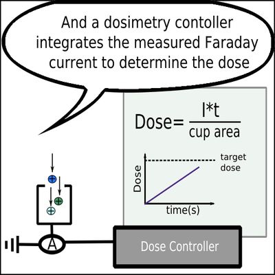 Dose accuracy in plasma doping
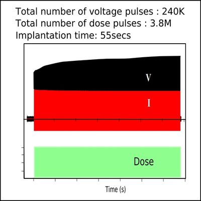 Implant pulse parameters to monitor plasma ion implantation systems for fault detection and process control
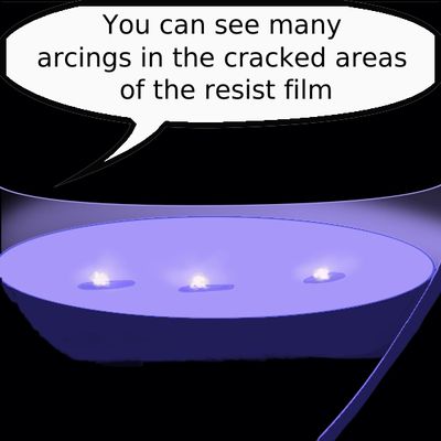 Simple and low cost test wafer for studying plasma induced wafer arcing damage
How to monitor plasma ion implantation process for fault detection?
Simple and low cost test wafer for studying plasma induced wafer arcing damage
How to monitor plasma ion implantation process for fault detection?
Leave a Reply